The fundamental building block of sequential logic
Prerequisites
This tutorial assumes familiarity with:
Binary numbers — understanding 0s and 1s, HIGH and LOW voltage levels
Logic gates (AND, OR, NOT) — basic combinational building blocks
Truth tables — how to read input/output relationships
No prior knowledge of sequential logic or timing is required — we’ll build that understanding here.
Why Do We Need Flip-Flops?
Combinational circuits have no memory — their outputs depend only on current inputs. But real digital systems need to:
Store data (registers, memory)
Count events (counters)
Track state (state machines)
Synchronize signals (clock domain crossing)
Flip-flops are the solution: they’re 1-bit memory elements that store a value until told to change.
Latch vs Flip-Flop
Before diving into flip-flops, let’s understand how they differ from latches.
What is a Latch?
A latch is a simple 1-bit memory element that is level-sensitive:
When the enable signal is HIGH, the latch is “transparent” — output follows input
When enable goes LOW, the latch “holds” — output stays frozen at its last value
The problem: while enabled, any input change immediately affects the output. This makes timing unpredictable in complex circuits.
The Key Difference
| Type | Triggered By | Behavior |
|---|---|---|
| Latch | Level (HIGH or LOW) | Transparent when enabled, holds when disabled |
| Flip-Flop | Edge (rising or falling) | Captures input only at the clock edge |
Flip-flops are preferred in synchronous design because:
Predictable timing — changes happen only at clock edges
Easier to analyze — one reference point per clock cycle
Avoids race conditions that plague level-sensitive latches
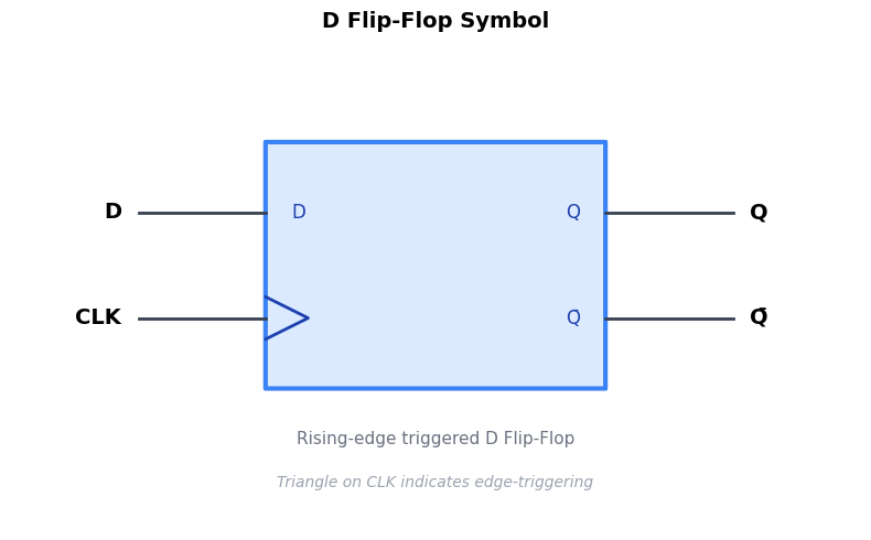
The D Flip-Flop
The D (Data) flip-flop is the most common type. It has:
D (Data input): The value to be stored
CLK (Clock): The timing signal that triggers capture
Q (Output): The stored value
Q̄ (Inverted output): The complement of Q — also written as /Q, Q’, or “NOT Q” (optional on many flip-flops)
Matplotlib is building the font cache; this may take a moment.
Truth Table
In truth tables for sequential circuits, Q(next) represents the value Q will have after the clock edge — the “next state” of the output.
| CLK | D | Q(next) | Description |
|---|---|---|---|
| ↑ | 0 | 0 | Captures 0 on rising edge |
| ↑ | 1 | 1 | Captures 1 on rising edge |
| — | X | Q | No edge → Q unchanged |
Key insight: Q only changes at the rising edge (↑) of CLK. At all other times, Q holds its value regardless of what D does.
How to Read a Timing Diagram
Throughout this tutorial, we’ll use timing diagrams to visualize flip-flop behavior. Here’s how to read them:
The basics:
Horizontal axis = Time (progressing left to right)
Vertical axis = Signal value (LOW=0 at bottom, HIGH=1 at top)
Each row = One signal (labeled on the left: CLK, D, Q, etc.)
Vertical dashed lines = Clock edges (reference points)
Signal shapes:
Square wave (CLK): Alternates HIGH/LOW periodically
Step changes: Signal transitions from one level to another
Flat sections: Signal holding steady
Reading tip: At each rising clock edge, note D’s value — that’s what Q will become. The clock edge is the cause; Q capturing D is the effect.
Edge-Triggered Behavior
The defining characteristic of a flip-flop is edge triggering. Let’s visualize this with a simple example:
D=1 before edge 1: Shows a value that IS captured at the rising edge
D=1 between edges 1-2: Shows that changes between clock edges are IGNORED
D=1 stable across edges 3-4: Shows normal capture of a stable signal
The core principle: only the value of D at the exact moment of the rising edge matters.
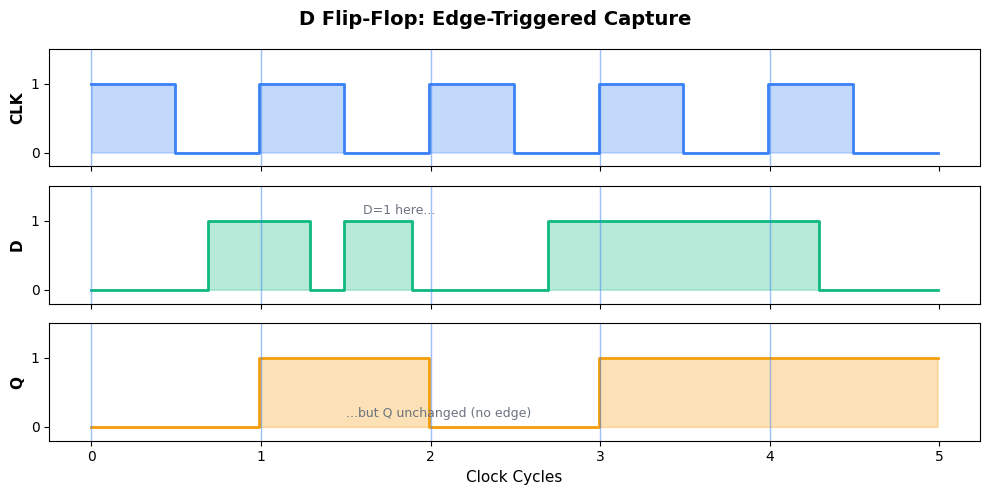
Notice:
D can change freely between clock edges — Q ignores it
Q only updates at rising edges, capturing whatever D was at that instant
Q holds its value until the next rising edge
Timing Parameters
For reliable operation, flip-flops have critical timing requirements. Let’s zoom in on a single clock edge to understand them:
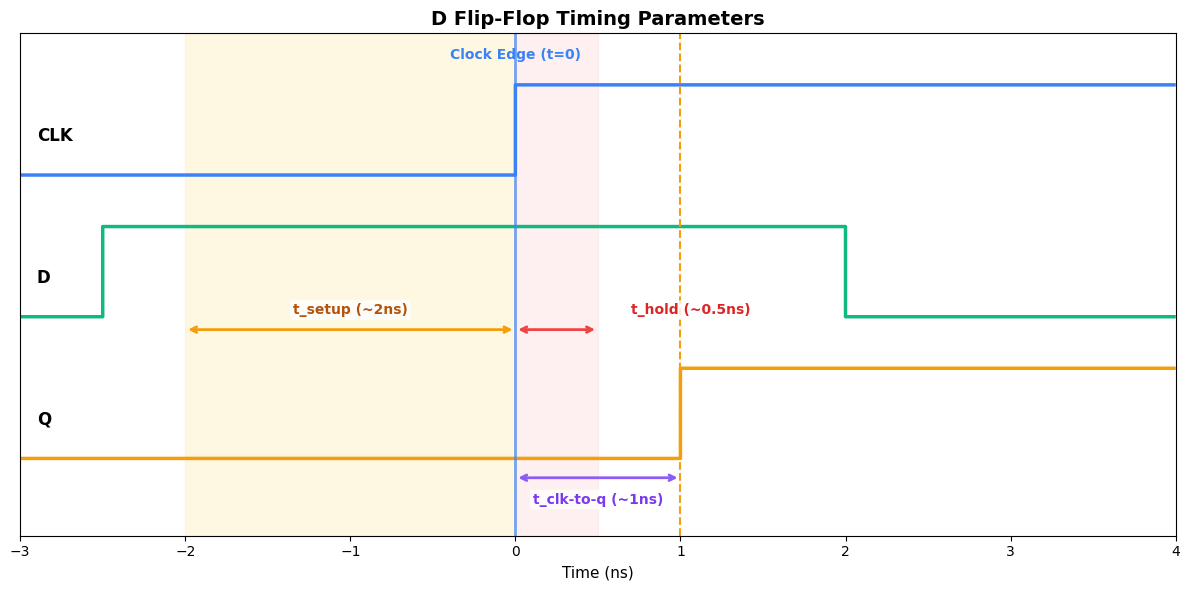
Key Timing Parameters
| Parameter | Symbol | Description | Typical Value |
|---|---|---|---|
| Setup time | t_setup | D must be stable before clock edge | 0.1-2 ns |
| Hold time | t_hold | D must remain stable after clock edge | 0.05-0.5 ns |
| Clock-to-Q | t_clk-to-q | Time from clock edge to Q change | 0.1-1 ns |
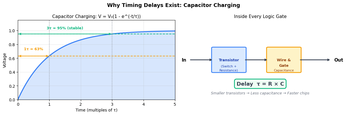
Why do these exist?
Flip-flops are built from transistors, and transistors aren’t instant switches. The delays come from charging and discharging tiny capacitors inside the chip:
Setup time — The flip-flop’s internal nodes (tiny capacitors formed by transistor gates and wires) need time to charge or discharge to stable voltage levels before the clock edge samples them. If D is still changing, the internal voltages are unstable and the flip-flop may latch an undefined value.
Hold time — When the clock edge arrives, the flip-flop begins “closing the gate” between input and output. During this brief transition, the input still has some influence on the internal nodes. D must stay stable until the isolation is complete.
Clock-to-Q — After latching the value internally, the output transistors must switch state. This means charging/discharging the output node capacitance through the transistor’s resistance. The delay follows τ = RC (resistance × capacitance).
In short: Every signal change requires moving electrons to charge capacitors. This takes time — typically picoseconds to nanoseconds depending on the capacitance and the transistor’s drive strength.
What happens if you violate these?
Setup violation: D changes too close to clock edge → Q might capture wrong value
Hold violation: D changes too soon after clock edge → Q becomes metastable (indeterminate state)
Who ensures timing is correct?
The circuit designer is responsible, with help from Electronic Design Automation (EDA) tools:
Static Timing Analysis (STA): Tools automatically check every path in your design and report violations before you fabricate the chip
For setup violations (most common):
Reduce the clock frequency (more time for signals to settle)
Shorten combinational logic paths by adding pipeline stages
Use faster logic gates
For hold violations:
Add delay buffers to slow down fast paths
Usually less common because gates have inherent delay
In practice, you design your circuit, run STA, fix any reported violations, and repeat until clean.
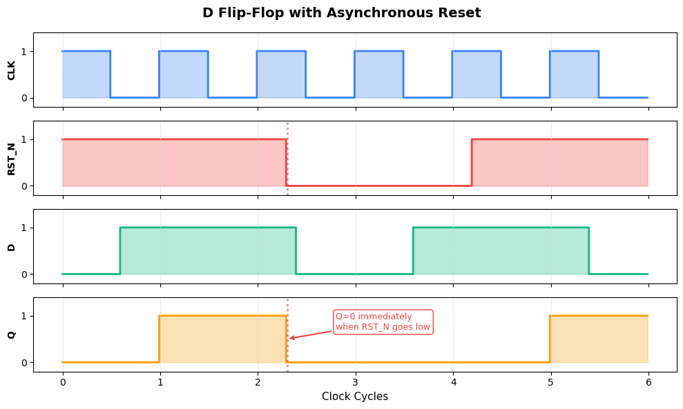
D Flip-Flop with Reset
Most flip-flops include a reset input to initialize to a known state. Two types exist:
Asynchronous Reset
Resets Q immediately when asserted, regardless of clock
Higher priority than clock
Can cause timing issues if not handled carefully
About the example timing: The signals were chosen to highlight asynchronous behavior:
RST_N asserted at cycle 2.3 (mid-cycle): Notice Q goes to 0 immediately — it doesn’t wait for a clock edge. This is the defining characteristic of async reset.
RST_N released at ~cycle 4.2 (also mid-cycle): Normal operation resumes at the next clock edge
D has values during reset: Even though D=1 during cycles 4-5, Q stays 0 because reset has priority
After reset: Q captures D normally starting at edge 5
The key insight: asynchronous means “ignores the clock” — reset takes effect the instant it’s asserted.
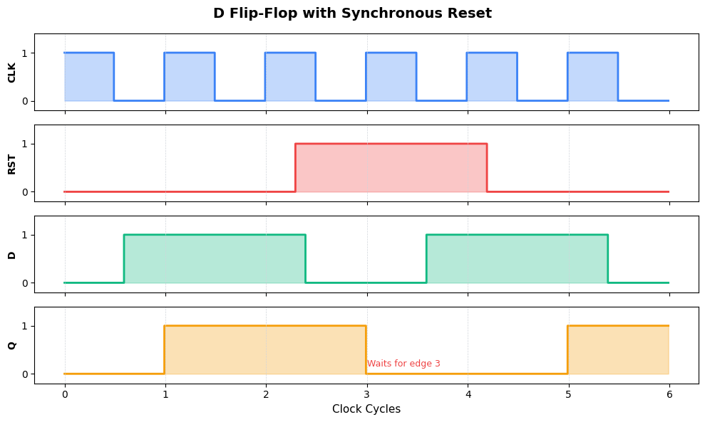
Synchronous Reset
Resets Q only at the clock edge when reset is asserted
Cleaner timing behavior
Preferred in most modern designs
About the example timing: Compare this directly to the async reset above — same D pattern, same reset window:
RST asserted at cycle 2.3 (mid-cycle): Unlike async, Q does NOT immediately go to 0. Q was 1 at edge 2, and it stays 1!
Q resets at edge 3: Only when the clock edge arrives AND reset is still active does Q go to 0
Reset still active at edge 4: Q stays 0 because reset overrides D
Normal operation at edge 5: Reset was released at ~4.2, so now D is captured normally
The key difference: Q stays at 1 from edge 2 until edge 3, even though reset was asserted at 2.3. Synchronous reset respects clock boundaries.
Comparison:
| Aspect | Asynchronous | Synchronous |
|---|---|---|
| Reset timing | Immediate | At clock edge |
| Priority | Higher than clock | Same as data |
| Timing analysis | More complex | Simpler |
| Use case | Power-on reset | Normal operation |
D Flip-Flop with Enable
An enable input allows you to selectively update the flip-flop.
About the example values:
D pattern
[1,0,1,0,1,0]: Alternating values to clearly show when D is captured vs ignoredEN pattern: High at edges 0, 1, 4, and 5 (two separate update windows)
Why this matters — trace through the diagram:
Edges 0 and 1 (EN=1): Q follows D → captures 1, then 0
Edges 2 and 3 (EN=0): D changes to 1, then 0, but Q stays at 0 (its last captured value)
Edges 4 and 5 (EN=1): Q captures again → gets 1, then 0
The Q values [1,0,0,0,1,0] follow directly from the rule: “capture D when EN=1, hold when EN=0”.
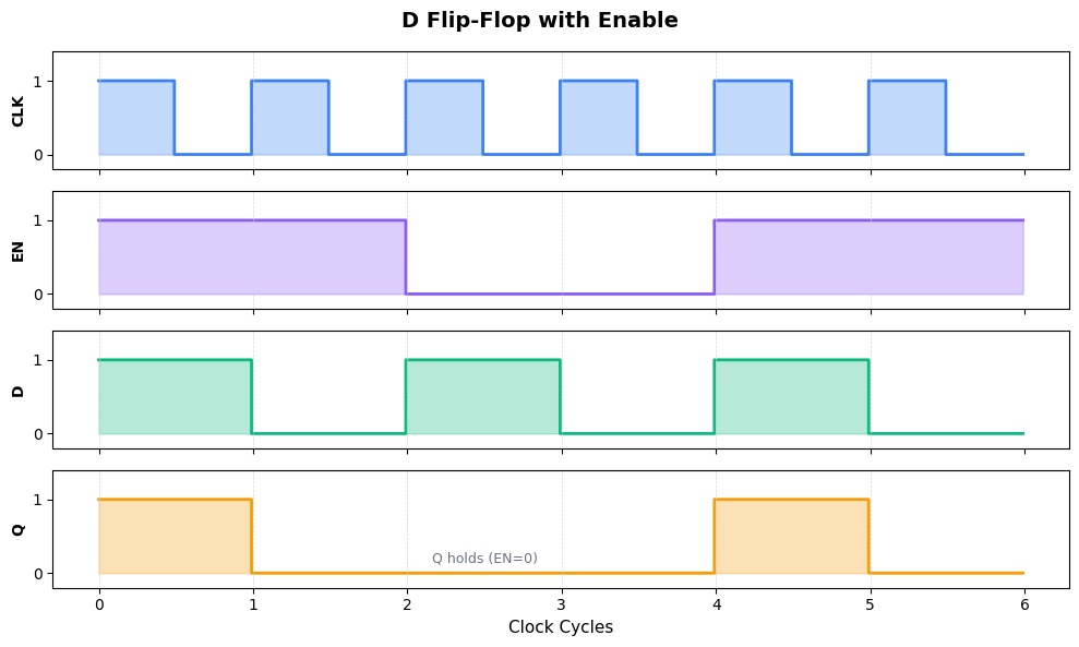
Enable behavior:
EN=1 at clock edge: Q captures D (normal operation)
EN=0 at clock edge: Q holds its current value (D ignored)
Use cases:
Selective register updates
Building larger registers with load enable
Power saving (clock gating)
Building Registers from Flip-Flops
A register is simply multiple flip-flops sharing the same clock, storing multi-bit values:
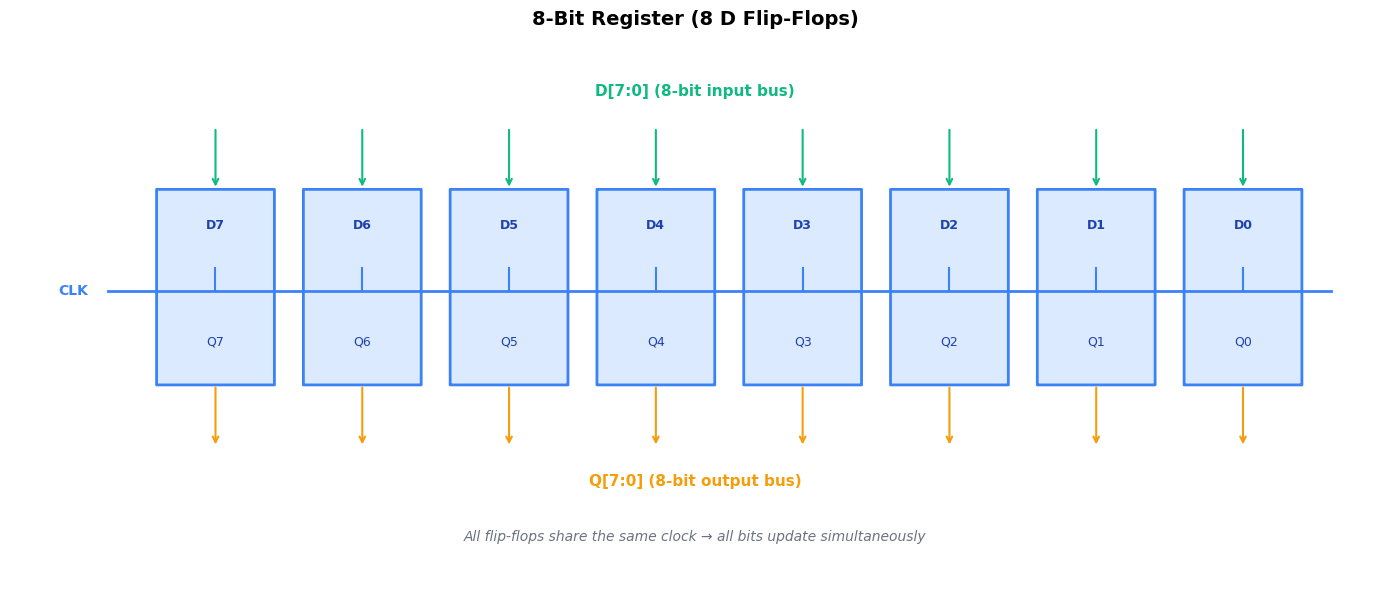
Register properties:
All bits update atomically at the same clock edge
Adding enable creates a “load” function
Adding reset initializes all bits to 0 (or preset to 1)
Common widths: 8, 16, 32, 64 bits
Common Applications
Data Storage — Registers hold values between operations in processors and digital systems. Every CPU register (like the program counter, instruction register, or general-purpose registers) is built from flip-flops. When you read “32-bit processor,” those are 32 flip-flops working together to store each register value.
Pipelining — Flip-flops separate pipeline stages, allowing multiple operations in flight simultaneously. Modern CPUs break instruction execution into stages (fetch, decode, execute, memory, write-back), with registers between each stage. This lets the CPU work on five different instructions at once, dramatically increasing throughput.
Counters — Chained flip-flops with feedback create binary counters for timers, frequency dividers, and address generation. A 4-bit counter cycles through 0→1→2→...→15→0 by connecting each flip-flop’s Q output to the next flip-flop’s clock input. These are everywhere: timers in microcontrollers, clock dividers in PLLs, and memory address counters.
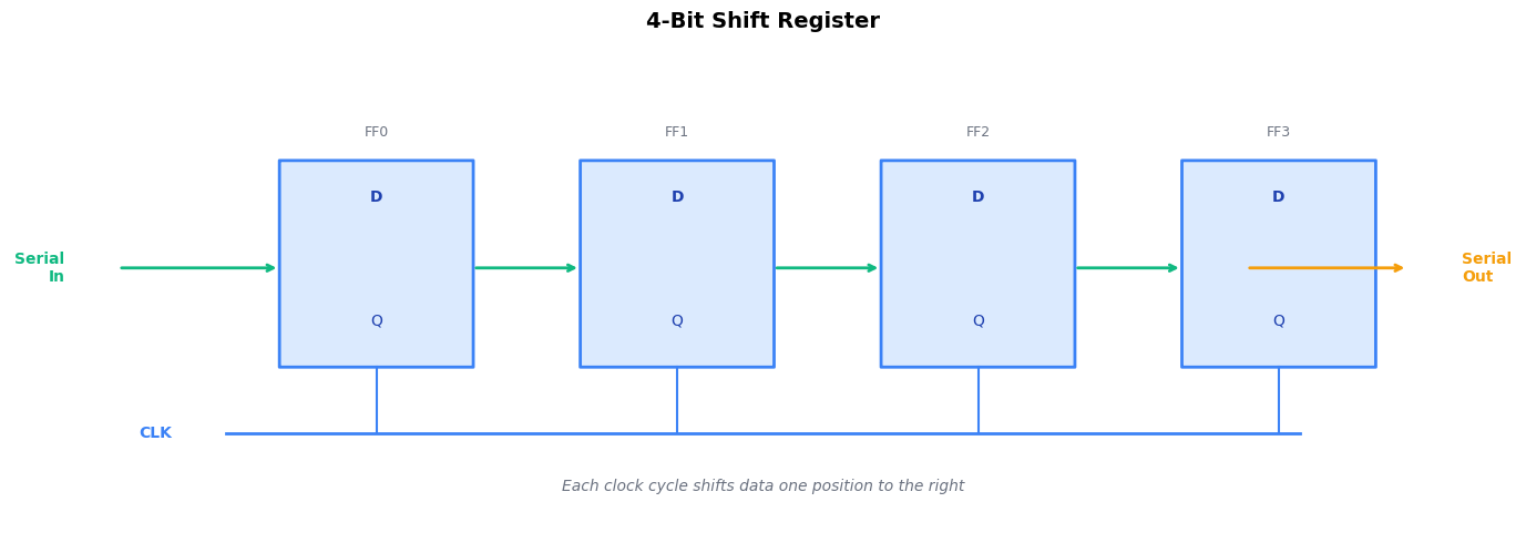
Shift Registers — Serial-to-parallel or parallel-to-serial conversion for data transmission and signal processing. By connecting flip-flops in a chain (Q of one feeds D of the next), data “shifts” one position per clock cycle. Used in serial communication (UART, SPI), LED matrix control, and implementing delays in signal processing.
Key Takeaways
D flip-flops are 1-bit memory elements — the building block of all sequential logic
Edge triggering is key — Q only changes at clock edges, providing predictable timing
Timing parameters matter:
Setup time: Data must arrive before the clock edge
Hold time: Data must stay stable after the clock edge
Clock-to-Q: Output delay after the clock edge
Reset options:
Asynchronous: Immediate, for power-on
Synchronous: At clock edge, cleaner timing
Enable allows selective updates — Q holds when disabled
Registers are just multiple flip-flops sharing a clock
Every counter, state machine, processor register, and memory cell uses flip-flops. Master the D flip-flop, and you’ve mastered the atom of digital memory.