Understanding signal behavior in multi-component systems
Prerequisites
This tutorial assumes you have completed:
D Flip-Flops in Digital Design — including how to read basic timing diagrams, edge-triggered capture, setup/hold times, and propagation delay
You should also be familiar with:
Binary numbers and logic levels (HIGH/LOW, 1/0)
Logic gates (AND, OR, NOT) and their behavior
What This Tutorial Covers
The D flip-flop tutorial taught you to read timing diagrams for a single component. This tutorial extends that skill to system-level timing diagrams involving multiple signals working together:
Signal types and notation — buses, active-low signals, conventions
Input/output perspectives — understanding whose view you’re looking at
Multi-signal coordination — memory interfaces, handshaking protocols
Pipeline timing — overlapped operations
Timing hazards — glitches and how to avoid them
These skills are essential for reading datasheets and debugging real hardware.
Anatomy of a Timing Diagram
Let’s start with a simple timing diagram showing a clock and a data signal.
About the example data: The data pattern [0, 0, 1, 1, 1, 0, 1, 0] was chosen deliberately to show:
Staying low (cycles 0-1): Data can remain stable across multiple cycles
Rising transition (cycle 2): LOW→HIGH change
Staying high (cycles 2-4): Data holds its value
Multiple transitions (cycles 5-7): Demonstrates that data can change every cycle
This pattern gives you a representative sample of the behaviors you’ll encounter in real timing diagrams.
Matplotlib is building the font cache; this may take a moment.
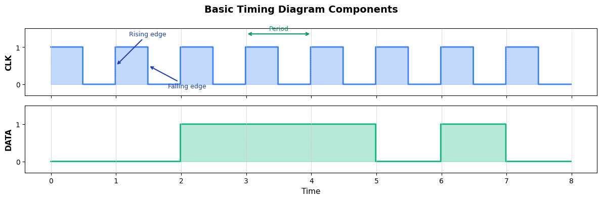
Key elements:
| Element | Description |
|---|---|
| Signal name | Label on Y-axis (CLK, DATA, etc.) |
| Logic levels | HIGH (1) and LOW (0) positions |
| Time axis | Horizontal axis showing progression |
| Rising edge | Transition from LOW to HIGH (↑) |
| Falling edge | Transition from LOW to HIGH (↓) |
| Period | Time for one complete clock cycle |
Signal Types in Timing Diagrams
Digital systems use several types of signals, each with distinct characteristics.
Important: Inputs vs Outputs
Timing diagrams show signals from the perspective of a specific component. Before reading any timing diagram, ask: “What component am I looking at?”
Inputs: Signals coming into the component from external sources
Outputs: Signals generated by the component
In the example below, imagine we’re looking at a data processing module:
| Signal | Direction | Source |
|---|---|---|
| CLK | Input | Crystal oscillator or PLL on the board |
| RST_N | Input | Power-on reset circuit (hardware that monitors power supply) |
| EN | Input | A controller or state machine that decides when this module should operate |
| D | Input | Upstream logic (e.g., a FIFO, another module’s output, or external pins) |
| BUS[7:0] | Output | This module’s result — downstream logic will read it |
About the example signals:
CLK: Input from the system clock generator — every synchronous component receives this
RST_N (active-low reset): Input from the power-on reset circuit. The timing (0.3 to 1.8) represents:
Starts at 0.3 (not exactly 0): The reset circuit needs time to detect stable power
Releases at 1.8: Released after power and clock are confirmed stable
This is asynchronous to the clock — notice it doesn’t align with clock edges
EN (enable): Input from a controller state machine that orchestrates the system. The controller asserts EN when it wants this module to process data (cycles 2-7), then deasserts it when done.
D (data): Input from upstream logic — could be a sensor interface, a FIFO buffer, or another module’s output. The pattern shows data arriving while the module is enabled.
BUS[7:0]: Output produced by this module. The slanting “X” lines at transitions are standard notation meaning:
All 8 bits are changing simultaneously
The “X” pattern says “transition happening — don’t sample during this time”
Values shown (
XX,00,01, etc.) are the stable values between transitionsXXat startup means “unknown” — the module hasn’t produced valid output yet
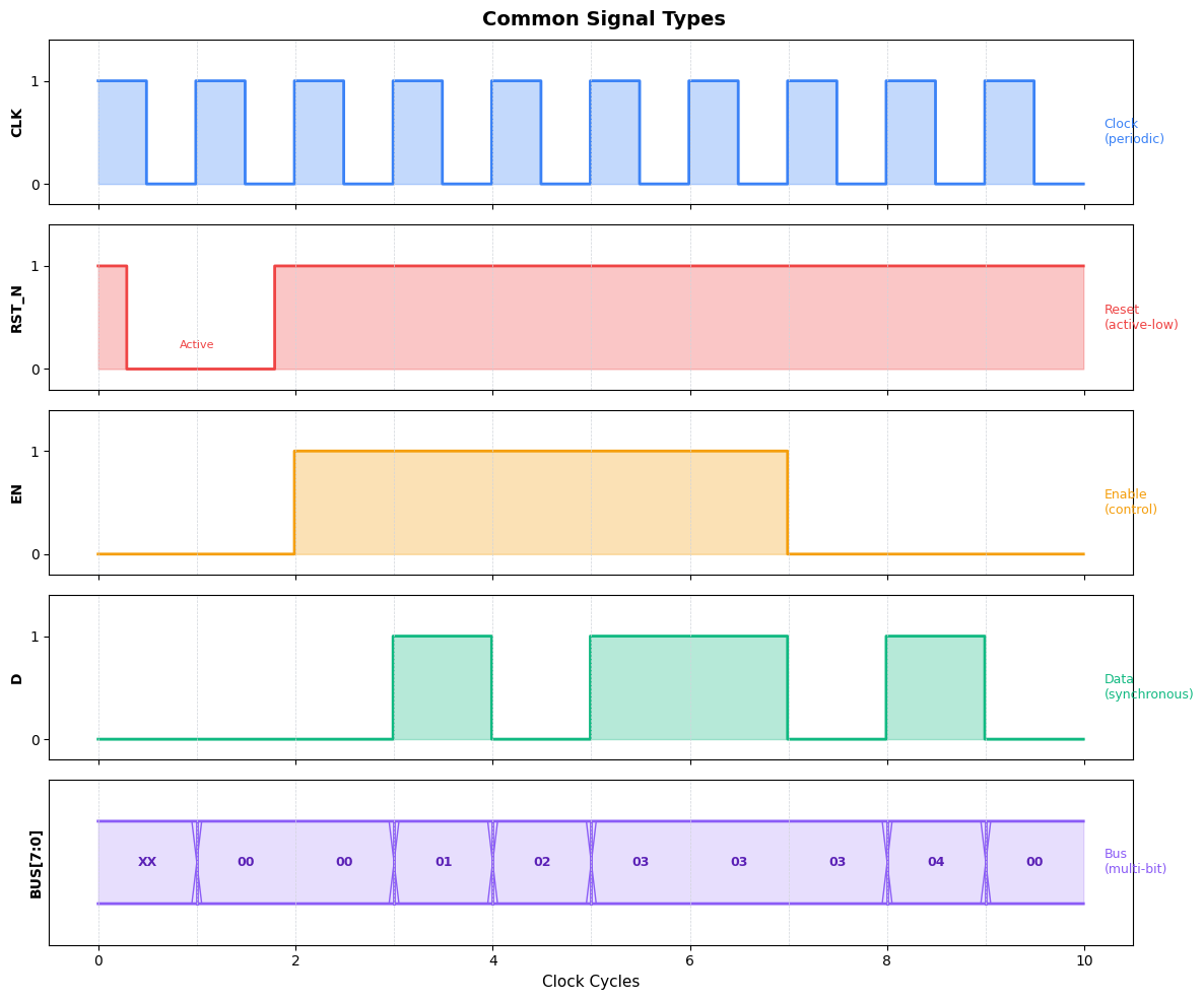
Signal type characteristics:
| Type | Characteristics | Examples |
|---|---|---|
| Clock | Periodic, fixed frequency | CLK, SYSCLK |
| Reset | Often active-low, assertion clears state | RST_N, RESET |
| Enable | Gates operations on/off | EN, CE, OE |
| Data | Changes relative to clock | D, Q, DATA_IN |
| Bus | Multi-bit values shown as hex/decimal | ADDR[15:0], DATA[7:0] |
Example: Reading a Memory Interface
Let’s examine a realistic timing diagram for a simple synchronous memory read operation.
About the signal timing: This example models a typical synchronous SRAM read sequence:
CS_N (Chip Select): Goes low at cycle 2 and stays low through cycle 6 — the memory chip ignores all other signals when CS_N is high
RD_N (Read Enable): Asserted one cycle after CS_N (cycle 3) — this is the actual read command
ADDR: Set to address
00when CS_N goes low — we’re reading from memory address 0x00DATA: Returns
42after one cycle delay (cycle 4) — memory needs time to fetch the dataVALID: Goes high when data is ready — tells the controller “you can sample now”
Why these specific values?
Address
00is simple — any address would work the same wayData value
42(the “answer to everything”) is memorable and clearly shows valid data vs high-impedanceZZOne-cycle latency between RD_N assertion and data valid is typical for synchronous memory
The
ZZ(high-impedance) shows the data bus is not being driven when no read is active
Reading this timing diagram:
Cycle 2: Address is placed on bus, chip select asserted (CS_N goes low)
Cycle 3: Read enable asserted (RD_N goes low)
Cycle 4: Memory responds with data, VALID goes high
Cycles 4-5: Data is valid — controller samples it on the rising edge
Cycle 6: Read complete, signals deasserted
Notation conventions:
ZZ: High-impedance (tri-state, bus not driven)
--: Don’t care (value irrelevant)
_N suffix: Active-low signal
Common Timing Diagram Patterns
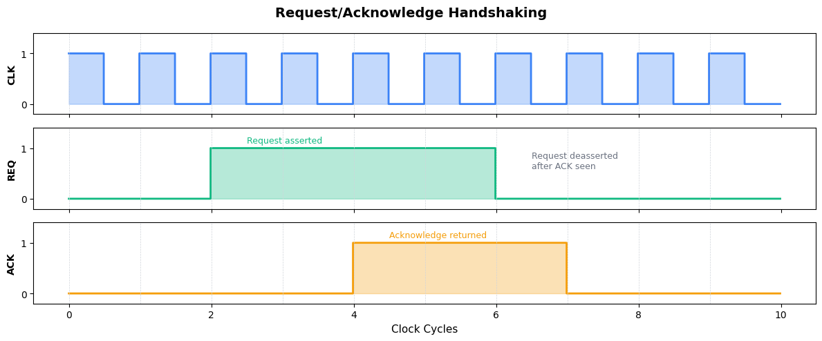
Pattern 1: Handshaking (Request/Acknowledge)
About the signal timing: This pattern shows a classic “four-phase handshake”:
REQ asserts (cycle 2): Requester says “I need something”
ACK asserts (cycle 4): Responder says “Got it, working on it” — the 2-cycle delay represents processing time
REQ deasserts (cycle 6): Requester sees ACK, says “Okay, I’ll wait”
ACK deasserts (cycle 7): Responder finishes, ready for next request
Why these specific timings?
2-cycle delay before ACK: Shows that the responder needs time to process (could be memory access, computation, etc.)
REQ held until ACK seen: Demonstrates proper protocol — you don’t drop your request until acknowledged
ACK held one cycle after REQ drops: Shows clean completion of the handshake
This pattern is fundamental — you’ll see it in bus protocols, FIFO interfaces, and inter-module communication.
Pattern 2: Pipeline Stages
About the example: We show 5 instructions (A, B, C, D, E) flowing through a 3-stage pipeline (Fetch → Decode → Execute).
Why these specific values?
3 stages: The minimum to show pipeline behavior clearly — real CPUs have 5-20+ stages, but the principle is the same
5 instructions: Enough to show:
Pipeline filling (cycles 1-3): Each cycle adds one more instruction in flight
Steady state (cycles 4-5): All 3 stages busy simultaneously
Pipeline draining (cycles 6-7): Last instructions completing
Letters A-E: Simple labels that make it easy to track each instruction’s progress through stages
Key insight to notice: Look at cycle 5 in the diagram — at that single instant:
Instruction C is being fetched
Instruction B is being decoded
Instruction A is executing
This “overlap” is why pipelines improve throughput — we’re doing 3 things at once instead of waiting for each instruction to fully complete.
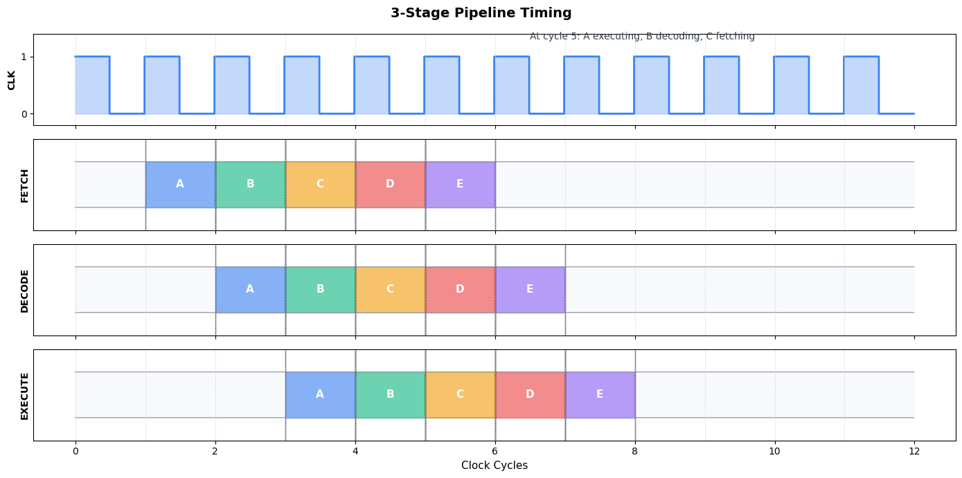
Pipeline insight: At any given cycle, multiple instructions are in flight simultaneously:
Each stage processes a different instruction
One instruction completes per cycle (after the pipeline fills)
Latency = 3 cycles, but throughput = 1 instruction/cycle
Timing Hazards and Issues
Glitches
A glitch is an unwanted short pulse caused by unequal propagation delays through different logic paths.
About this example: We use the simple logic function Y = A AND (NOT B) with a specific input change designed to expose the glitch:
Why A=0→1 and B=0→1 simultaneously?
In the ideal world (zero delay): When both go from 0 to 1:
A becomes 1, B becomes 1, so NOT B becomes 0
Y = 1 AND 0 = 0 (no change from initial state)
In the real world: The NOT gate has a small delay (~0.1 time units in our example)
A rises to 1 immediately
NOT B is still 1 (hasn’t processed B’s change yet)
For that brief moment: Y = 1 AND 1 = 1 → GLITCH!
Why this matters: This specific input transition (both inputs changing together) is the classic “static hazard” case. The glitch duration equals the NOT gate’s propagation delay. In a real circuit, this could:
Cause a downstream flip-flop to capture the wrong value
Trigger unintended state machine transitions
Corrupt data in asynchronous designs
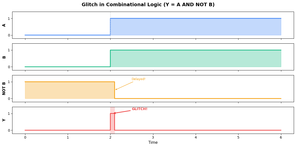
Why glitches occur: When A and B both change from 0→1:
Ideally: Y stays 0 (since A·B̄ = 1·0 = 0)
Reality: A rises immediately, but NOT B takes time to fall
Brief moment: A=1, NOT B=1 (hasn’t updated yet) → Y=1 (glitch!)
Avoiding glitch problems:
Register outputs to sample only at clock edges
Use synchronous design practices
Add glitch filters for asynchronous inputs
Key Takeaways
Timing diagrams are essential for understanding and debugging digital circuits
Clock edges are reference points — in synchronous design, everything happens relative to the clock
Setup and hold times define when data must be stable for reliable capture
Propagation delay limits how fast your circuit can run
Common notation:
Active-low signals: _N suffix or overbar
High-impedance: Z or Hi-Z
Don’t care: X or --
Bus transitions: X-crossing pattern
Practice reading timing diagrams from datasheets — they’re the universal language of digital hardware
Timing diagrams bridge the gap between abstract logic design and physical hardware reality. Master them, and you’ll be able to debug the most challenging timing issues.